The four fundamental forces of Nature
The contemporary Physics recognizes four fundamental types of forces in Nature. Of these four, we only experience the presence of two in our daily lives: The force of gravity (why does everything fall toward Earth? Why does Earth rotate Sun?) and the Electromagnetic force. The latter is responsible for almost any kind of force that we experience in our daily lives besides gravity. For example, lightning, the fact that we can walk, the heartbeat, all chemical reactions, computers, and everything that we know relies on the presence of electromagnetic force.
Computers are not an exception to the prevalence of electromagnetic force. The flow of electricity in computer hardware makes them work and be capable of processing and storing data.

How do computers process and store data?
Computer hardware relies on the force of electromagnetism to store and process data. Specifically, they use electric voltage and electricity flow or the lack of flow to store and process data as a sequence of 0 and 1. The transistor is the fundamental building block of a modern conventional computer’s central processor unit (CPU). Transistors were invented in the early 1950’ and are switches that can control or amplify an electric current. The inner workings of a transistor are displayed in the figure below.
Each transistor has three components:
- Base: The base controls whether current is allowed to flow through the transistor when power is applied.
- Collector: When there is the power to the base, the collector current is allowed to flow toward the emitter.
- Emitter: The emitter takes the electric current that the collector is allowed to send to be used on other parts of your circuit.
Combinations of transistors can build the electronic equivalents of the logical operators we discussed in DATA 1301: Introduction to Data Science, for example: AND, OR, NAND, NOR, XOR, XNOR. Then, the combinations of these logical operators can become equivalent to addition, subtraction, multiplication, and other more complex operations.
What is the relevance and importance of transistors?
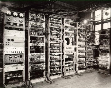
In the early days of computers, around and before 1950, computers were mostly fixed-program computers, a kind of computer that had to be rewired to perform a new task. Even nowadays, we still have these kinds of computers around us, like calculators. As such, the early computers tended to be big, costly, hard to program and slow. Soon, scientists and engineers realized that this computer programming approach was infeasible for most tasks as it was tedious and complex.
The turning point in the history of computers was the invention of transistors which enabled the development of microchips. Microchips, also called Integrated Circuits (IC) are sets of electronic circuits on a small flat pieces of silicon. On each IC, many transistors act as miniature electrical switches that can turn a current on or off.
The following figures schematically illustrate how a transistor acts as a switch or amplifier: The flow of a tiny amount of current in the base activates the flow of a major current through the collector to the emitter and out of the transistor.
The modern computer architecture
With the invention of transistors, many scientists and engineers independently proposed and devised alternative architectures (to fixed-program computers) that stored the instructions to act on data along with the data in the memory instead of physically implementing the tasks in the hardware and rewiring the hardware for new tasks. The computer would then read the program (the set of instructions to perform) from memory and execute the instructions.
The idea of a stored-program computer as described above was introduced in the late 1940s by the famous scientist John Von Neumann, who proposed that a computer program be electronically stored in binary-number format in a memory device so that instructions could be modified by the computer as determined by intermediate computational results.
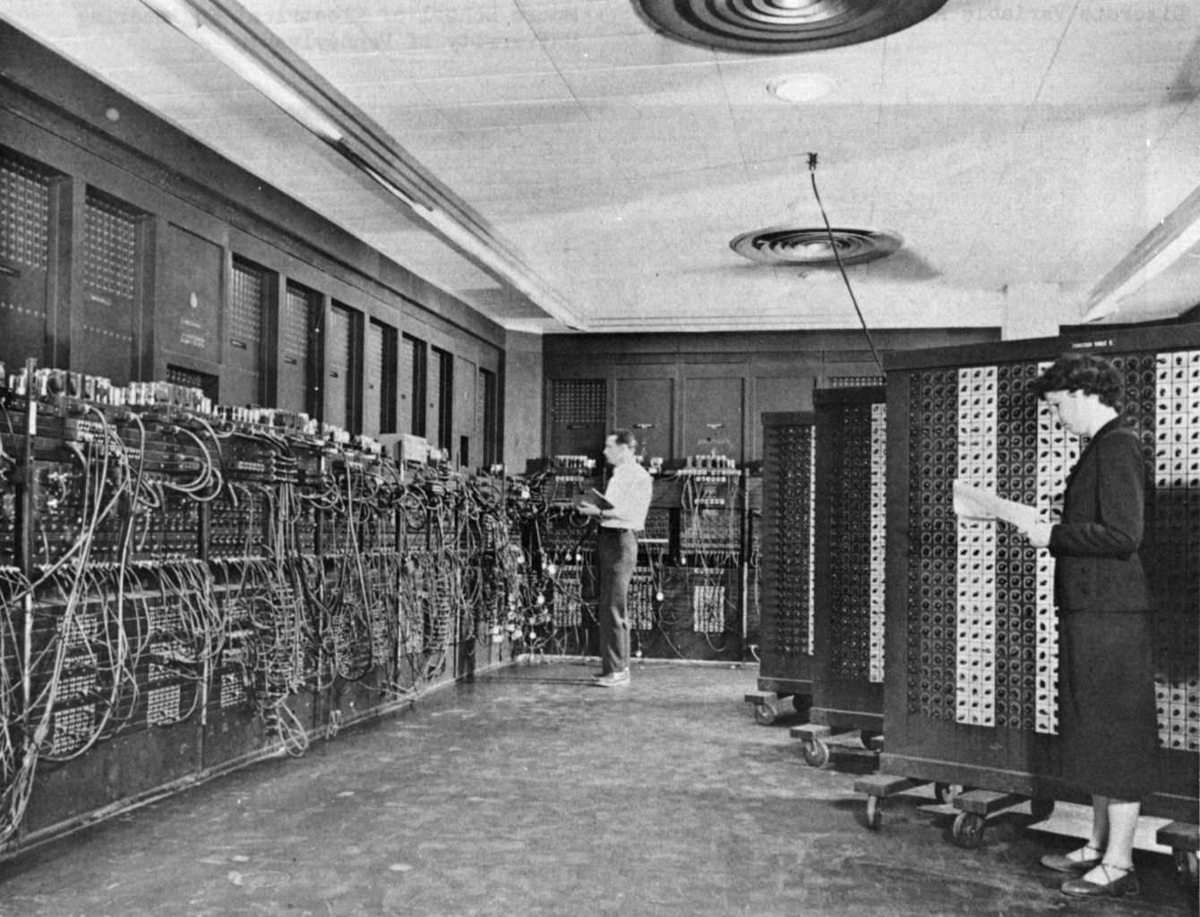
Two of the earliest examples of stored-program computers are ENIAC and Manchester Mark 1.
One such stored-program computer architecture that has become popular and remains so to this date is the Von Neumann Architecture proposed by John Von Neumann.
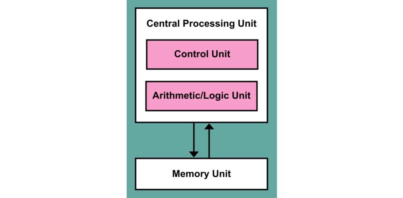
The Von Neumann computer architecture, displayed in the above figure, has the following major components:
- Memory array (MEM) holds all the commands (instructions) and numbers (data).
- Control Unit:
- Program counter selects which instruction to execute from a special type of memory called instruction registers. The counter normally increases just by 1 in each step.
- Arithmetic block performs arithmetic operations (
+,-, …) on the input data (comprised of binary 0 and 1). The input/output of the arithmetic block are held in a special part of computer memory called CPU registers.
The instructions the CPU has to execute are typically of two types: data instructions and control instructions. Each data instruction contains four parts:
- two addresses specifying which two operands to pick from the memory (MEM).
- one command that specifies what operation to perform.
- the memory location to store the result of the operation.
The CPU Cycle
The Central Processing Unit (CPU) is a major component of all modern computers which is responsible for processing all data and instructions in the computer. From the moment you switch a computer on to the moment you shut it down, the computer CPU recycles through three tasks:
- The instruction fetch stage, during which a new instruction is fetched from the memory address that is currently stored in the Program Counter (PC) and stored into the instruction register. At the end of the fetch operation, the PC points to the next instruction that will be read at the next cycle.
- The decode stage during which the encoded instruction presented in the instruction register is interpreted by the CPU decoder.
- The execute stage during which the control unit of the CPU passes the decoded information as a sequence of control signals to the relevant functional units of the CPU to perform the actions required by the instruction, such as reading values from registers, passing them to the Arithmetic Logic Unit (ALU) to perform mathematical or logic functions on them, and writing the result back to a register. If the ALU is involved, it sends a condition signal back to the control unit (CU). The result generated by the operation is stored in the main memory or sent to an output device. Based on the feedback from the ALU, the PC may be updated to a different address from which the next instruction will be fetched.
The computer performs the above three tasks sequentially and repeatedly until it is shut down. A single repetition of the three tasks by the CPU is called an instruction cycle (also known as the fetch–decode–execute cycle, or simply the fetch-execute cycle, or more famously known as the CPU Cycle).
The number of cycles that the CPU can perform in one second is one of the most popular measures of the CPU speed, famously known as the CPU clock rate or the CPU Clock Speed. The clock speed measures the number of cycles your CPU executes per second, measured in GHz (gigahertz). In this case, a cycle is the basic unit that measures a CPU’s speed. During each cycle, billions of transistors within the processor open and close. This is how the CPU executes the calculations contained in the instructions it receives. For example, a CPU with a clock speed of 2.8 GHz executes 2.8 billion cycles per second.
What does determine the computer speed?
Since the early days of invention of transistors, engineers realized that as the transistors get smaller, their power consumption also reduces proportionally, such that the overall Power Density of transistors remains roughly the same. For example, reducing the size of a transistor by about 30% would also,
- reduce the electronic device usage area by $\sim50%$,
- reduce the capacitance associated with the device by $\sim30%$ (thus reducing electric current latencies and transition times),
- reduce the voltage by $\sim30%$ while keeping the current the same.
The above factors would then collectively,
- increase the operating frequency the transistors by $\sim40%$, and
- decrease the power consumption $\sim50%$.
This observation has become known as the Dennard scaling, also known as MOSFET scaling in honor of Robert H. Dennard who was a co-author of a 1974 paper discussing this semi-empirical phenomenon.
The Dennard Scaling implies that the more transistors we can fit on an Integrated Circuit (IC), typically of size 1 centimeters, the faster the CPU will become. Short after the discovery of Dennard Scaling, Gordon Moore, the former CEO of Intel, predicted in 1975 that the transistor count in microprocessors will double every two years. His prediction held for multiple decades to become known as Moore’s law.
The following graph shows the number of transistors in various CPUs manufactured over the past decades. For several decades, the Dennard Scaling and Moore’s Law were the drivers of CPU performance.
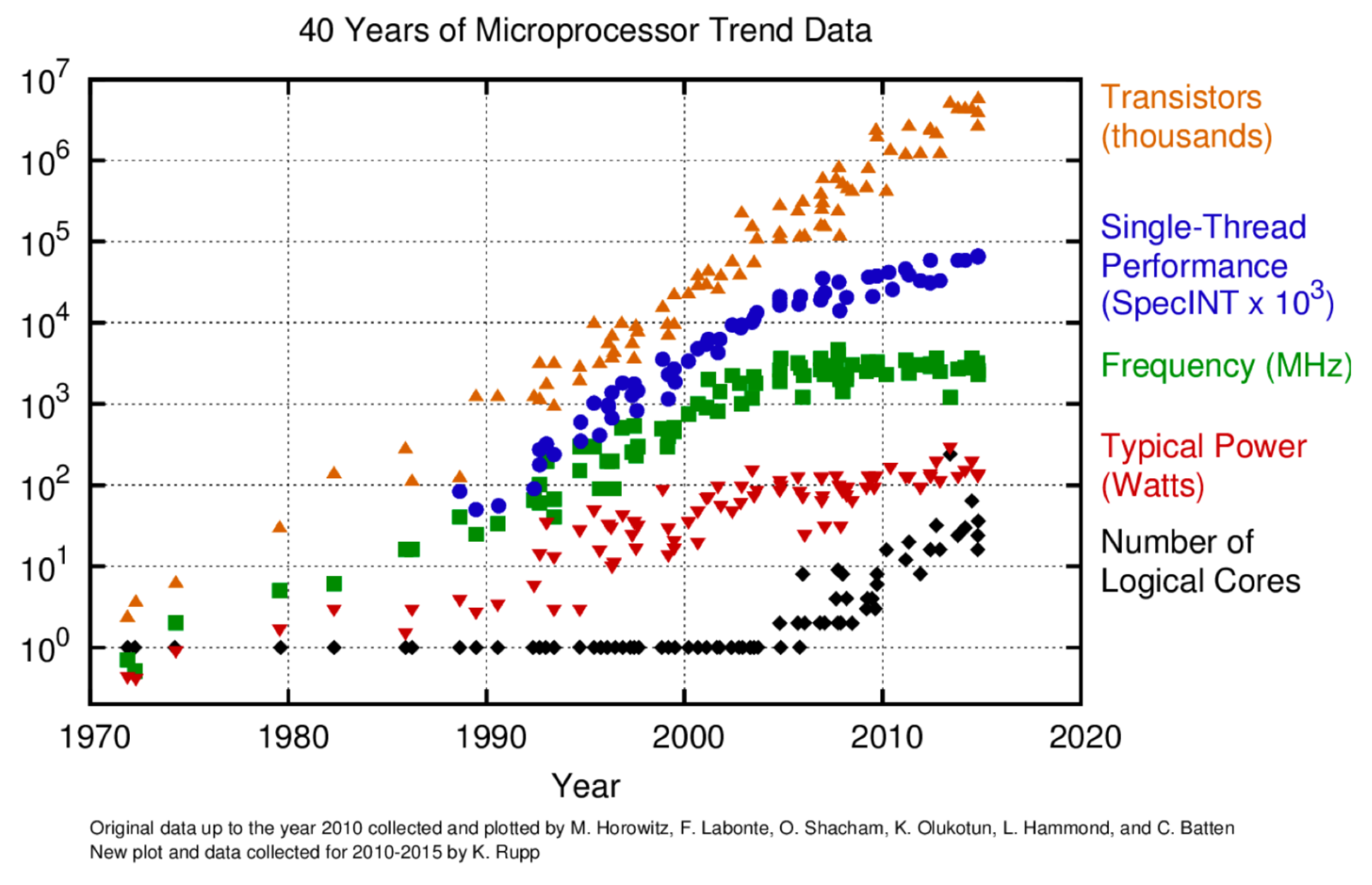
However, this strategy of speeding up CPUs by shrinking and adding more transistors to Integrated Circuits began to fail with the start of the new millennium, around 2005: The transistors had become so small that they did not function properly in the circuits; the circuit features became so small that their magnetic fields had noticeable impact on the movements of electrons in other part of the circuit, causing unnecessary heating and occasional bit flipping (A bit is the tiniest piece of data in computers).
As such, the increase in the number of transistors gradually slowed down during the 2000s. Instead of speeding up CPUs by adding more transistors, manufacturers started to focus on getting more useful computing tasks done in a single CPU cycle. In other words, instead of making transistors ever smaller, manufacturers focused on getting more tasks done with the same transistors that are reshaped for better concurrency and parallel efficiency. Such an ambitious goal was achieved by, for example,
- Overlapping the execution of CPU instructions so that different parts of the CPU are kept busy (pipelining),
- Executing operations without necessarily waiting for the previous ones to complete (speculative and out-of-order execution),
- Adding multiple execution units to process independent operations concurrently (superscalar processors or SISD operations),
- Increasing the machine word size (i.e., the number of bits that the computer’s CPU can process in one go, for example, 32bits or 64bits), to allow a Single Instruction to be applied concurrently to Multiple Data (SIMD operations),
- Creating a memory hierarchy of varying sizes and efficiency levels to speed up memory access time (CPU register/cache),
- Adding multiple identical computing cores on a single chip (shared-memory parallel computing),
- Using multiple CPUs in a single node (distributed-memory parallel computing),
- Designing custom hardware to solve specific problems with better and faster (e.g., Application-specific integrated circuits (ASICs), Field-programmable gate arrays (FPGAs)).
The computer memory hierarchy
In the early days of computers, the performance of CPU and memory access were about the same. While memory was extremely limited, the speed bottleneck was typically the CPU. However, the rapid technological progress in the development of smaller transistors led to the design of CPUs that became increasingly faster than the typical memory access speed of the time.
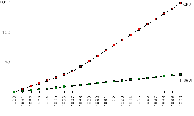
As such, the performance bottleneck in modern computers is frequently the memory access and not the CPU speed. To partially address this speed gap between CPU and memory, manufacturers design contemporary computer architectures with a hierarchical memory structure with varying sizes and speeds. This is in contrast to design of memory as a single homogeneous chunk of data storage available to the processor.
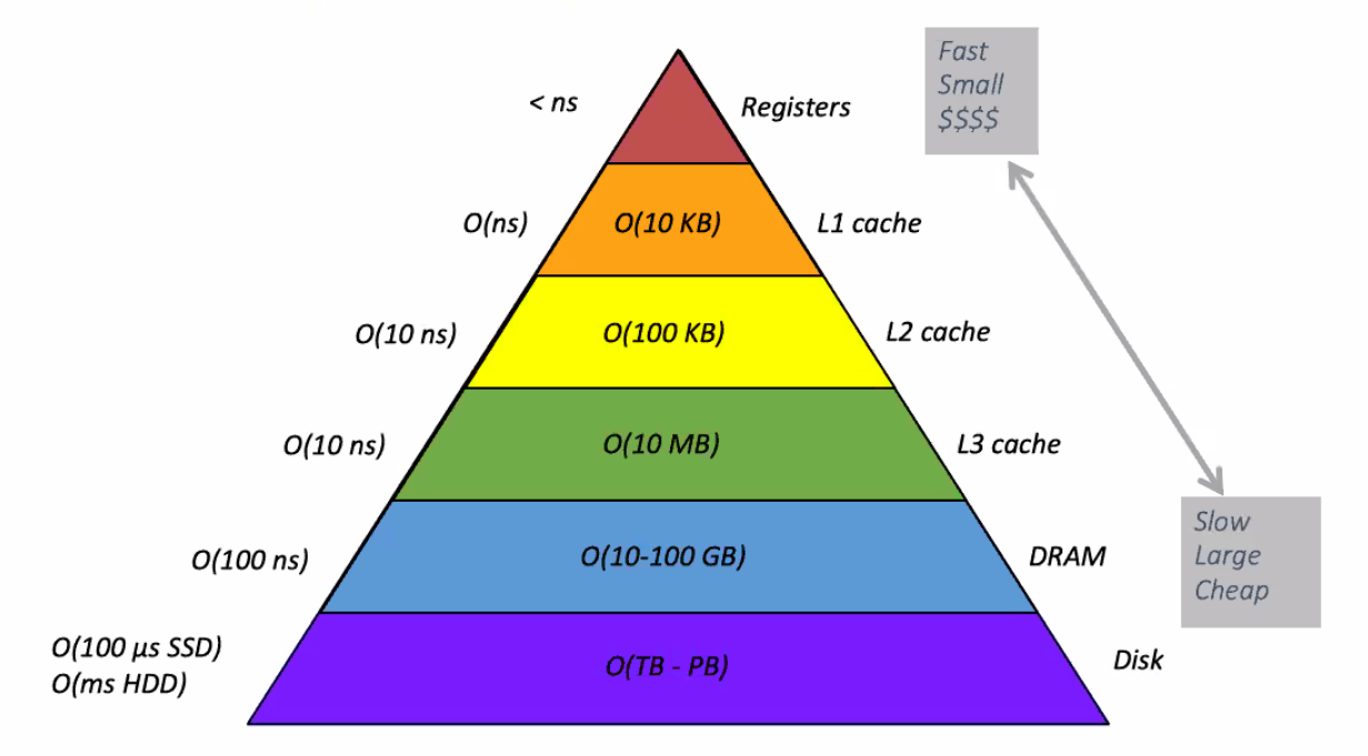
In this hierarchy, as we move to the tip of the pyramid, closer to the processor, the memory access speed increases. However, the memory size also shrinks. There is, therefore, a compromise between memory access speed and memory size.
The benefit of this hierarchical memory layout is that the CPU can predict and prefetch the future data or instructions from the slower but larger levels of memory hierarchy to the higher levels for subsequent usage by the CPU for computations.